PCB SURFACE FINISHING :Direct Immersion Gold (DIG)
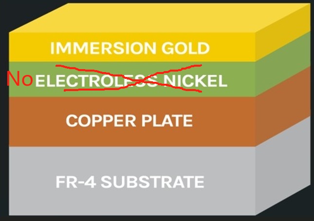
DIG Direct Immersion Gold is a nickel-free PCB surface finish that deposits an autocatalytic gold layer directly onto the copper. Unlike the more common Electroless Nickel Immersion Gold (ENIG), which places a nickel barrier between the copper and the gold, DIG eliminates this intermediate layer.
How the DIG process works
Preparation: The copper surface of the PCB is thoroughly cleaned and prepped.
Auto-catalytic deposition: The board is submerged in an electroless gold plating bath. Unlike a displacement reaction, where gold is exchanged for copper, this autocatalytic reaction deposits gold without corroding the underlying copper.
Resulting finish: The process creates a dense, uniform, and ductile gold layer directly on the copper, providing a protective, bondable, and solderable surface.

Advantages and Disadvantages of Direct Immersion Gold (DIG)
I. Advantages
Nickel-free, avoiding the risk of "black pad":Direct Immersion Gold (DIG) eliminates the nickel barrier layer in the traditional Electroless Nickel Immersion Gold (ENIG) process, fundamentally avoiding the "black pad" failure problem. This issue is caused by the embrittlement and oxidation of the nickel layer, which easily leads to fragile solder joints and reduced connection reliability. The nickel-free design of DIG completely eliminates this hidden danger.
Superior solder joint reliability:During the soldering process, the direct copper-gold interface in DIG forms a stable copper-tin intermetallic compound (Cu₆Sn₅). Compared with the intermetallic compound formed at the nickel-tin interface in the ENIG process, the structure of Cu₆Sn₅ is more stable, has stronger fatigue resistance, and can effectively reduce the generation of microcracks, significantly improving the long-term reliability of solder joints.
Suitable for fine-pitch component packaging:The DIG process can form a flat and uniform gold layer surface. For fine-pitch layouts (such as high-density PCBs) and components (such as Ball Grid Arrays, BGAs) that have extremely high requirements for pad flatness, this surface characteristic can ensure the alignment accuracy and contact stability during soldering, reducing the risks of virtual soldering and bridge soldering.
Better high-frequency performance:Nickel is magnetic and easily causes signal loss due to the "skin effect" in high-frequency scenarios. The nickel-free characteristic of DIG can avoid this problem, reduce signal attenuation, and is therefore more suitable for high-frequency electronic devices such as radio frequency (RF) and microwave devices that have strict requirements for signal integrity.
Compatible with wire bonding process:Whether it is gold wire or aluminum wire bonding, the DIG surface treatment can provide a reliable bonding effect, and no additional high-temperature treatment is required. Stable bonding can be achieved in a room temperature environment, meeting the packaging requirements of components that need wire connection, such as semiconductor chips and sensors.
Higher environmental compliance:DIG is a lead-free process, which fully complies with the EU RoHS (Restriction of Hazardous Substances in Electrical and Electronic Equipment) and environmental regulations in other regions. There is no need to worry about market access issues caused by excessive lead content.
II. Disadvantages
Relatively high costGold, as a precious metal, has a high raw material cost. Although the DIG process has fewer steps than ENIG (eliminating the nickel layer deposition step), its overall cost is still at a relatively high level compared with non-gold surface treatments such as Lead-Free Hot Air Solder Leveling (HASL) and Organic Solderability Preservatives (OSP). It may lack cost-effectiveness for mid-to-low-end consumer electronic products that are sensitive to cost.
Poor wear resistance:The gold layer formed by DIG is relatively thin (usually 0.1-0.5 μm) and has a soft texture, resulting in weak wear resistance and inability to withstand repeated plugging, unplugging, or friction. For example, the edge connectors of circuit boards (commonly known as "gold fingers") need to frequently contact the slots. If DIG treatment is used, problems such as gold layer wear and copper exposure oxidation are likely to occur. Therefore, it is not suitable for such scenarios that require high wear resistance.
Limited storage shelf life:Although the DIG surface has good stability under standardized storage conditions (such as vacuum packaging and normal temperature dry environment), when exposed to the air for a long time, the gold layer may still oxidize slowly, resulting in reduced surface solderability. Compared with OSP (usually with a storage period of more than 6 months), the effective storage period of DIG is shorter, and the time connection between production, storage, and assembly needs to be controlled.
Direct Immersion Gold (DIG) Application Scenarios
Direct Immersion Gold (DIG) is particularly suited for applications requiring high reliability, excellent electrical performance, and tight pitch precision. These include:
High-Frequency Communication Devices: Devices operating in high-frequency bands can leverage gold’s superior electrical properties to enhance performance.
Flexible PCBs: Gold’s good ductility makes it an ideal surface finish for flexible PCBs—these boards need to withstand bending and folding without damage.
High-Density Interconnect (HDI) Boards: HDI boards feature fine lines and spaces, and the precision and reliability offered by DIG perfectly meet their strict requirements.
As an experienced PCB manufacturer, I-tech electronics co., ltd has mature Direct Immersion Gold (DIG) capabilities. We precisely control gold layer uniformity and adhesion, with the full process (from nickel-free design to final inspection) meeting standards—ideal for fine-pitch components and high-frequency devices.
We’ve delivered custom DIG PCBs to communications and semiconductor clients, earning recognition for no "black pad" risks and low high-frequency signal loss. For your DIG PCB needs, i-tech offers end-to-end support (design to mass production) to boost your product’s reliability and performance.


