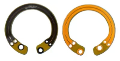
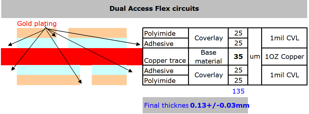
Dual Access Flex PCB Dual access flex PCBs are flexible circuits that can be accessed from both the top and bottom surfaces, yet feature only a single layer of conductor trace. Coverlay openings are present on both sides of the flex circuit, enabling solderable PADs on the top and bottom. Although it may seem similar to a double - sided FPC, the stack - up of a dual - access flex circuit board differs due to its single copper trace. As a result, there's no requirement for a plating process to create plated through holes (PTH) for connecting the top and bottom sides, and the trace layout is considerably simpler.
Application
Vibration Motor for Mobile Phone
- LCD Module for Mobile Phone
Printer
Advantages of Dual Access Flex PCB
1. Two - Sided Connection without Through - Holes
Dual - access flex PCBs allow for connection on both sides directly through the copper layer. In contrast, a 2 - layer FPC requires the creation of through - holes to establish electrical connections between the two sides. This absence of through - holes simplifies the manufacturing process, reduces potential points of failure, and can lead to a more reliable circuit in certain applications. For example, in applications where minimizing the risk of via - related issues (such as via resistance or via - hole cracking) is crucial, dual - access flex PCBs offer a distinct advantage.
2. Superior Flexibility and Bendability
Thanks to their simpler stack - up design, dual - access flex PCBs exhibit better flexibility and bendability compared to 2 - layer (2L) flexible circuits. The reduced complexity in the layer arrangement means there are fewer interfaces and materials to potentially impede bending. This makes them ideal for applications that require repeated or extreme bending, like in some wearable electronics or compact, flexible connectors within small - form - factor devices.
3. Versatile Soldering Pad Placement
The soldering pads on dual - access flex PCBs can be located anywhere on both the top and bottom sides. This provides greater design freedom for engineers. For instance, it allows for more creative component placement strategies, enabling better utilization of the board space. In complex circuit designs where components need to be placed in non - traditional positions for optimal functionality or to avoid interference, this feature of dual - access flex PCBs proves to be extremely valuable.
Disadvantages of Dual Access Flex PCB
1. Complex Production Process
The production process of dual - access flex PCBs is akin to that of 2 - layer flex circuits. However, it is more challenging and intricate. Due to limitations in production techniques, the manufacturability of dual - access circuit boards is restricted. For instance, the precise alignment and processing of the single - layer conductor trace while ensuring access from both sides demand highly specialized equipment and skilled labor, which are not always readily available or cost - effective.
2. Prone to Wrinkling and Tearing
The base material of dual - access flex PCBs is mainly copper, which is extremely thin. This thinness makes it highly flexible, but also difficult to keep flat during the manufacturing process. As a result, it is easy to tear. During the hot laminating process, wrinkles and blisters occur more frequently. For example, when the copper trace is subjected to heat and pressure during lamination, its soft and flexible nature causes it to buckle and form blisters, which can compromise the integrity of the final product.
3. Limited Component Placement
Only a small number of components can be placed on dual - access flex PCBs. The copper trace is relatively fragile, and if too many components are added, it is easy to break. For example, when components are soldered onto the board, the stress from the soldering process and the weight of the components can cause the thin copper trace to crack, leading to circuit failures.
In most cases, it is more practical to convert dual - access FPCs into 2 - layer FPCs. 2 - layer FPCs are simpler to manufacture and have the same cost. If you have any questions or need more information about dual - access flexible circuits, please feel free to contact I-tech today.


