PCB Engineering


 PCB Engineering Solution

I-tech Electronics works closely with various customers in a consulting capacity to ensure that circuit board specifications not only precisely match end-use scenarios but also align with the budget requirements of different clients. As a professional team in the printed circuit board (PCB) field, this customized consulting service is our core competitive advantage that distinguishes us from industry intermediaries. We are proficient in various PCB technologies, especially with rich practical experience in complex products such as rigid-flex PCBs. We are committed to helping customers enhance market competitiveness, shorten time-to-market, and accelerate new product development through close collaboration.
dc490ec101eea46666609f40a21f394.png


I-tech Electronics provides the following PCB engineering solutions and professional technical support to fully meet your needs and quality expectations:


1.Design Rule Check (DRC)

I-tech Electronics understands the importance of proactively controlling quality to avoid risks in the manufacturing process. Our rigorous and reliable Design Rule Check mechanism comprehensively verifies key parameters in the design. For rigid-flex PCBs, we also focus on checking special indicators to ensure structural stability.
General PCB Design Rule ChecksAdditional Checks for Rigid-Flex PCBs
Trace width and spacingPrecision of fillet processing at rigid-flex transition areas
Open/short circuits in netsCompliance of minimum bending radius of flexible parts
Aspect ratioAccuracy of coverlay window dimensions
Note: The table only lists core check items. Actual DRC also includes verification of other parameters affecting manufacturability (such as pad-to-hole size matching, solder mask bridge design, etc.) to minimize production errors from the design stage. If risks are identified, we will communicate immediately and provide alternative solutions.


2.Design for Manufacturability (DFM)

At I-tech Electronics, you will receive a fully optimized PCB design solution — we always refine designs around core elements such as cost, safety, compliance, time-to-market efficiency, reliability, and customer satisfaction.
General PCB DFM AnalysesAdditional Evaluations for Rigid-Flex PCBs
Drilling precisionConnection strength between rigid and flexible areas (e.g., copper foil bonding technology)
Annular ring integrityCompatibility between flexible area coverlay and lamination processes
Rationality of trace width and spacingRationality of component layout in folding areas (to avoid compression or mutual interference)
Hole alignment, solder mask quality, silkscreen clarity-

Note: DFM analysis covers all dimensions of circuit board layout. Beyond the items in the table, it also includes evaluations of details such as test point design, thermal path optimization, and mechanical strength adaptation, ultimately maximizing efficiency throughout the entire process from manufacturing to after-sales service.


3.Cost Consulting

Total product costs are affected by multiple factors such as materials and delivery cycles, with a wide range of fluctuations. We understand that enterprises need to strictly control costs in all links of the production chain. Our technical team will conduct in-depth discussions with customers on optimization solutions.
General PCB Cost Optimization ItemsAdditional Cost Control Items for Rigid-Flex PCBs
Material selectionOptimizing material thickness of flexible areas (e.g., streamlining unnecessary reinforcing layers)
Layer adjustment (addition/reduction)Adjusting the ratio of rigid to flexible areas
Drilling size optimizationOptimizing panel layout (considering folding and storage needs of flexible parts)
Trace width/spacing adaptation, panel layout schemes-

Note: Cost optimization must align with customer functional requirements and reliability standards. In addition to the items in the table, it also includes comprehensive suggestions on adjusting delivery cycles (balancing expediting costs) and simplifying process complexity.


4.Surface Finish Consulting

There are various surface finish options for printed circuit boards. Choosing the right solution can significantly improve assembly efficiency, which needs to be matched according to product requirements.
Common Surface Finish MethodsCore Application Scenarios
Electroless Nickel Immersion Gold (ENIG)High-reliability applications, fine-pitch components, wire bonding
Hot Air Solder Leveling (HASL)Cost-sensitive projects, general electronic assemblies (lead-free options meet RoHS compliance)
Immersion SilverHigh-speed circuits, applications requiring good solderability and flatness
Electroless Nickel Electroless Palladium Immersion Gold (ENEPIG)High-reliability, high-frequency, and wire bonding applications

Note: The selection of surface finishes must comprehensively consider factors such as product lifespan, storage environment, and assembly processes (e.g., reflow soldering temperature). Beyond the table, we can also provide customized suggestions for special scenarios (such as high-frequency signal transmission, outdoor weather resistance).


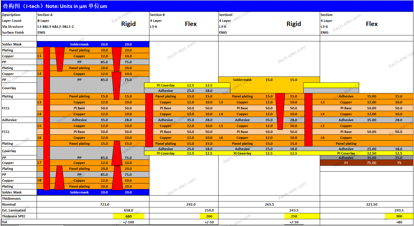
5.Stackup Design

PCB stackup design consists of copper layers, cores, and prepregs, requiring comprehensive consideration of cost, impedance characteristics, and anti-warping/anti-twisting performance. For rigid-flex PCBs, special attention is paid to material compatibility between rigid and flexible areas (such as smooth transition of copper foil thickness, balancing differences in substrate elastic modulus).


Note: In addition to impedance matching details not shown in the table, stackup design also includes signal/ground layer distribution, power integrity optimization, and interlayer alignment control. We can provide impedance models directly importable into your design software based on customer needs.


6.Laminate and Raw Material Selection Recommendations

Choosing the right laminate is crucial to ensuring end-product performance, which needs to be matched according to application scenarios:
Application ScenariosRecommended Materials
High-speed RF/microwave productsRogers (e.g., RO4000/5880 series), Taconic (e.g., TLX/TLY series, PTFE-based), Arlon (e.g., MT4000 series, PPO/PPS blends), Isola (e.g., IS620/680 series, cyanate ester resin)
5G high-frequency communication/mmWave applicationsLiquid Crystal Polymer (LCP), low-loss Polyimide (low loss PI), hydrocarbon resin (PCH, ceramic-filled modified)
Harsh environments (extreme temperatures)Polyimide or ceramic materials
General applicationsFR-4 based laminates (e.g., standard FR-4, mid-to-high speed FR-4 such as Shengyi S1000-2)
Rigid-flex PCBs (flexible areas)High bending-resistant polyimide (PI); copper foils matched to dynamic/static bending requirements
Note: Laminate selection must also consider parameters such as flame retardancy (e.g., UL94 V0) and dielectric constant stability (for high-frequency scenarios). For RoHS-compliant products, it is recommended to use materials with a glass transition temperature (Tg) > 140°C to withstand high-temperature assembly. High-frequency and high-speed materials are characterized by low dielectric constant (Dk) and low dissipation factor (Df), with different materials suitable for different frequency ranges: Rogers 5880 (Dk=2.2, Df=0.0009) and Taconic TLX (Dk=2.45, Df=0.0015) are suitable for millimeter waves (above 60GHz); Arlon MT4000 (Dk=3.5, Df=0.0025) and Isola IS680 (Dk=3.0, Df=0.0022) are suitable for 10-40GHz scenarios. LCP materials are widely used in 5G mobile antenna modules due to excellent high-frequency stability but require attention to shrinkage control; hydrocarbon resin (PCH) has a Df of approximately 0.0028 at 10GHz, offering a balance of cost and performance, suitable for high-layer count board designs.


7.Panelization Design

Optimizing panelization is a key link in PCB manufacturing. Our services can meet a wide range of needs — from standard rectangular, V-scored boards to complex routed and retained panel configurations.


Note: In addition to elements not shown in the table such as guide rails and fiducial markers, panelization design also includes optimization of details like depaneling methods (e.g., mouse-bite, laser cutting), board edge 留白尺寸,and anti-static design, balancing compatibility with automated assembly and production efficiency.


8.Controlled Impedance

For products requiring impedance control (single-ended signals, differential pairs, coplanar waveguides, etc.), we provide comprehensive support, including stackup guidance, custom design, and rigorous verification.


Note: Impedance control focuses on signal reflection management (rather than insertion loss). Content not covered in the table includes control of impedance tolerance ranges (e.g., ±10%) and impedance matching strategies for different signal types (high-speed digital signals, RF signals) to ensure signal integrity.


For customers launching new products with tight timelines and requiring complex PCBs, I-tech Electronics can more efficiently meet their time-sensitive needs through end-to-end technical support from prototype design to mass production.