
ENEPIG: A Superior PCB Surface Finishing Option
1. Definition and Basics
ENEPIG, which stands for Electroless Nickel Electroless Palladium Immersion Gold, is a surface finishing technique for PCB boards. Some engineers refer to it as ENIPIG. In both ENEPIG and ENIPIG, a layer of palladium is immersed between the nickel and gold layers. This palladium layer serves a crucial function: it prevents the mutual migration of nickel and gold, thereby eliminating the appearance of the dreaded "black pad" issue.
Both ENEPIG and ENIPIG possess several desirable properties. They exhibit strong wire bonding capabilities, excellent solder joint reliability, the ability to endure multiple reflow soldering cycles, and an extended storage time. As a result, they can meet a wide array of different assembly requirements.
The key difference between ENEPIG and ENIPIG lies in the plating thickness. When the palladium layer is thin, with a thickness ranging from 0.0125 - 0.02um (0.5 - 0.8u”), it is called ENIPIG. Conversely, when the palladium layer is thick, with a thickness between 0.05 - 0.5um (2 - 20u”), it is known as ENEPIG.
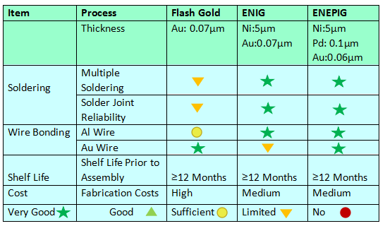
2. Features of ENEPIG Finish
3. ENEPIG Process
3.1 Oil Removal
Just like in other surface treatment processes, oil removal is the initial and vital step. This process aims to eliminate mild oil and oxides on the copper surface. By cleaning the copper surface, it increases wettability.
3.2 Micro Etching
Micro etching is a surface roughening process. Its functions include removing the oxide layer on the copper foil surface and etching away 1um - 2um of copper from the copper substrate surface. This increases the adhesion between the copper and the chemical nickel layer.
3.3 Acid Cleaning
Acid cleaning involves using an acid solution to remove scale and rust on the copper surface.
3.4 Sterling Predip
The pre - dipping process serves two main purposes. It maintains the acidity of the activation tank and ensures that the copper surface enters the activation tank in a fresh, oxide - free state.
3.5 Activation of Palladium
The activation solution contains ionic palladium. This step is crucial as the copper surface cannot be directly subjected to electroless nickel plating. Additionally, it is necessary to form a firmly - bonded palladium layer on the copper surface.
3.6 Chemical Nickel
To ensure solder reliability, the electroless nickel layer needs to have high ductility. The phosphorus content in the nickel layer is related to the weldability and corrosion resistance of the coating. Generally, the phosphorus content is required to be 7 - 9%. If the phosphorus content is too low, it can reduce the solderability and the strength of the soldering joint.
3.7 Chemical Palladium
A chemical palladium process is added between the chemical nickel and chemical gold processes to prevent the formation of black pads. Currently, the main components of the chemical palladium used by our company include PdCl2, NaH2PO2, the complexing agent ammonium hydroxide, the accelerator, and the stabilizer ammonium chloride, among others.
3.8 Chemical Gold
The chemical gold process is directly deposited on the chemical palladium layer. The mechanism is a displacement reaction, taking advantage of the large difference in electrode potential between the nickel - palladium and gold electrodes. Nickel and palladium can displace the gold ions in the plating solution. When the nickel or palladium surface is in contact with gold, the displacement reaction continues until the nickel or palladium layer is fully covered by the new gold layer, as the gold layer is porous.
4. ENEPIG vs ENIG and Flash Gold
4.1 Flash Gold
Flash Gold functions as a metal resist, being resistant to all common etching solutions. It has high electrical conductivity and is an ideal metal for corrosion resistance and for creating a contact surface with low contact resistance.
4.2 ENIG (Immersion Gold)
The immersion gold process uses a chemical oxidation - reduction reaction to form a gold coating. It deposits a nickel - gold coating on the PCB board surface that has a stable color, good brightness, a flat coating, and excellent solderability. Immersion gold enables the PCB to maintain good electrical conductivity during long - term use and has environmental tolerance that other surface treatment processes lack.
4.3 ENEPIG
Compared to ENIG, ENEPIG has an additional layer of palladium between the nickel and gold layers. During the replacement gold deposition reaction, the electroless palladium layer protects the nickel layer from excessive corrosion by the replacement gold.
5. ENEPIG PCB Advantage
In summary, compared to other surface treatment methods, ENEPIG offers several advantages. It has stable durability, excellent solder resistance, good compatibility, high coating flatness, and is suitable for high - density pads. As a result, it can be applied to more precise PCBs, and its welding performance is also superior.
ENEPIG was first proposed by Intel. Currently, many BGA boards are designed for gold bonding wire on one side and soldering on the other side. The thickness requirements for the gold plating layer on both sides differ. Bonding requires a thicker gold layer, approximately 0.3 microns or more, while soldering only needs about 0.05 microns. If the gold layer is too thick, soldering strength may be compromised, and if it is too thin, bonding may be ineffective. Previously, a dry film was used, and gold plating with different specifications was carried out twice to meet the requirements. Now, ENEPIG with the same thickness specifications on both sides can meet the bonding and soldering requirements. The current specifications for palladium and gold film thickness are around 0.08 microns or above, which can satisfy both bonding and soldering needs.
Currently, an increasing number of companies, such as Microsoft, Apple, and Intel, are widely using ENEPIG on PCB boards.