Via in Pad (VIP) PCB Technology: Applications, Advantages, and Challenges

1. Introduction to Via in Pad (VIP) in PCB Design
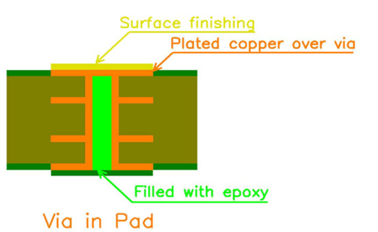
In PCB design, especially for small - sized PCBs with limited space around BGA (Ball Grid Array) components, the Via in Pad (VIP) technology is widely adopted. This technology enables vias to be plated and concealed beneath BGA pads. The PCB manufacturing process involves filling the vias with epoxy and then plating copper over them, making the vias essentially invisible.
2. Advantages of Via in Pad PCB Technology
Enhanced Trace Routing: Via in Pad significantly improves trace routing capabilities. It allows for more efficient signal routing in areas where space is at a premium, such as around BGA components. This results in a more compact and organized PCB layout.
Improved Thermal Dissipation: VIP technology aids in thermal dissipation. The vias can act as heat paths, transferring heat from components to other layers of the PCB more effectively. This is crucial for maintaining optimal operating temperatures, especially in high - power - consuming devices.
Reduced Inductance in High - Frequency Boards: In high - frequency boards, the use of Via in Pad helps to reduce inductance. By providing a more direct electrical connection, it minimizes the inductive effects that can interfere with high - speed signal transmission, thus improving the overall performance of the PCB in high - frequency applications.
Flat Component Surface: It offers a flat surface for component placement. This is beneficial as it ensures better contact between the component and the PCB, enhancing the mechanical and electrical stability of the assembly.
3. Disadvantages of Via in Pad
Higher Cost: Due to its complex manufacturing process, Via in Pad PCBs are more expensive compared to normal PCBs. The additional steps of epoxy filling and subsequent copper plating add to the production costs.
Solder - Off Risk: In cases where low - quality materials or manufacturing processes are used, there is a risk of solder - off from the BGA pad. This can lead to poor electrical connections and ultimately, product failures.
4. Technical Principle of Via in Pad
The inner - layer holes are first plugged with resin and then pressed together. This technique effectively resolves the conflict between controlling the thickness of the bonded dielectric layer and the inner - hole filling design.
5. Applications of Via in Pad
HDI Products: The use of via - in - pad plugging resin is widespread in HDI (High - Density Interconnect) products. It meets the design requirements for a thin dielectric layer, which is essential for achieving high - density circuitry in modern electronic devices.
Inner - Layer Buried and Blind Holes: For the design of buried and blind holes in the inner layer, an inner resin - filling process is often required. This is because the middle - layer dielectric design may be partially thin, and resin filling helps to ensure proper electrical and mechanical integrity.
Large - Blind - Hole Products: In some products where the thickness of the blind hole is greater than 0.5mm, it is impossible to use pressing adhesive to fill the hole. In such cases, resin plugging is necessary to fill the vias and prevent issues such as blind holes without copper.
6. Production Process
The production process of Via in Pad PCBs typically involves the following steps:
Laminate Shear: The laminate material is cut to the appropriate size.
Drilling: Holes are drilled for the vias and other necessary connections.
P.T.H. (Plated - Through - Hole): The drilled holes are plated with copper to create electrical connections.
Panel Plating: The entire panel is plated to ensure uniform coverage.
Resin Plugging: The vias are filled with resin.
Polishing: The surface is polished to create a smooth finish after resin plugging.
PTH Drilling: Additional holes may be drilled if required.
P.T.H.: Another round of copper plating for the newly drilled holes.
Panel Plating: Re - plating of the panel.
Outer Layer Image: The outer - layer circuit pattern is transferred.
Pattern Plating: Selective plating of the circuit pattern.
Etching: Unwanted copper is etched away.
S/M Coating (Solder Mask Coating): A solder mask is applied to protect the circuit.
Surface Finishing: The surface is finished, e.g., with a coating for corrosion resistance or improved solderability.
Routing: The PCB is cut to its final shape.
Test: The PCB is tested for electrical integrity.
Backpacking & Shipping: The PCBs are prepared for shipment.
7. Prevention and Improvement Measures for Via in Pad Problems
Ink Management: Use appropriate ink and strictly control its storage conditions and shelf - life. This helps to prevent issues related to the ink used in the process, such as poor adhesion or incorrect curing.
Inspection for Voids: Implement a standard inspection procedure to detect voids in pad holes. Even with excellent technology and optimal conditions, there is still a small (1/10000) chance of voids occurring, which can lead to scrap. The only way to address this is by identifying the location of void - containing holes and attempting repairs. Currently, there is no ideal equipment to completely solve the problem of detecting resin - plugged hole voids.
Resin Selection: Choose the proper resin, paying close attention to the material's glass transition temperature (Tg) and expansion coefficient. Also, ensure the use of appropriate production processes and removal parameters. This can prevent the separation of the pad from the resin after heating, which is a common issue in Via in Pad manufacturing.
Copper Thickness Control: Regarding the problem of delamination between the resin and copper, it has been found that when the thickness of the copper on the hole surface is greater than 15um, the delamination issue can be significantly improved.


