Embedded Copper Block (Coin)

Embedded Copper Block (Coin) PCB Technology: Thermal Dissipation Characteristics and Process Optimization
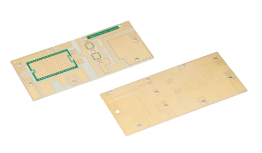
                                      image.png

1. Technical Background and Application Value

With the increasing demand for PCB thermal dissipation capacity in high-density electronic components and high-power devices, the industry has introduced embedded copper block (Coin)PCB technology. This technology utilizes the high thermal conductivity of copper blocks (thermal conductivity: 401 W/m·K) to rapidly transfer heat generated by internal components to the copper block, which then dissipates heat through air convection. The process involves: after completing the circuit layer fabrication and lamination of the PCB, creating mounting cavities via slot milling and wall metallization, and finally embedding the copper block into the slots. The copper block and PCB achieve physical fastening through embedding tolerance and electrical connection through copper plating, forming an efficient heat dissipation pathway. This article analyzes and optimizes the technology from three aspects—copper block design, dimensional compensation, and pressing control—to enhance the quality and reliability of PCB products.

2. Technical Classification and Thermal Advantages

According to the bonding method between the copper block and PCB, the technology can be divided into buried copper block(coin) PCB and embedded copper block(Coin) PCB:


  • Embedded Copper Block (Coin)PCB: The copper block is inserted into pre-milled and metallized slots after PCB lamination. Mechanical fastening is achieved through embedding tolerance, and electrical conduction relies on electroplated copper layers on the slot walls.

  • Buried Copper Block(Coin) PCB: The copper block is embedded into pre-milled grooves during the lamination process, with interlayer bonding realized via prepreg.


Performance Comparison:


Indicator

Embedded Copper Block(Coin) PCBBuried Copper Block(Coin)PCB

Thermal Efficiency

+30% (shorter heat transfer path)

Baseline

Process Steps

Reduced by 2-3 steps

More complex lamination procedures

Cost

15%-20% lower

Higher material consumption


The embedded copper block design directly contacts the inner copper layers and external air, forming a "component-copper block-air" heat dissipation channel, which improves thermal efficiency by ~30% compared to the buried type. Additionally, the reduced process steps lower costs by 15–20%, offering broader application prospects. However, immature technology and process challenges easily cause reliability issues, limiting large-scale adoption.

3. Process Challenges and Failure Modes

The core process of embedded copper blocks—"slot milling-metallization-embedding"—faces critical technical challenges:


  1. Copper Block(Coin) Structural Design Flaws
    Poorly designed geometries can cause mismatches with slots, leading to damage to the copper block or slot walls, with scrap rates potentially reaching 25%.

  2. Dimensional Tolerance  (Out-of-Control)

    • Inadequate compensation between slot and copper block dimensions causes excessive gaps (>0.2 mm) or interference (<-0.05 mm), increasing thermal contact resistance or mechanical stress.
    • Non-compliant flatness (CS surface >±100 μm, SS surface >±150 μm) results in uneven thermal interface material (TIM) thickness, reducing heat dissipation efficiency by 20–40%.
  3. Unstable Pressing Processes
    Uneven pressure or uncontrolled pressing speed can cause copper block displacement (>0.1 mm) or plating cracks (>0.5 mm).

4. Process Optimization Solutions

(1) Copper Block Structure and Dimensional Design

  1. Geometry Optimization

    • Adopt a tooth-shaped structure with rounded edges:
      • Tooth height: 0.2 mm ± 0.05 mm (enhances mechanical interlock, pull-out force ≥50 N);
      • Rounded edge radius: 0.2 mm ± 0.05 mm (reduces stress concentration, slot wall damage rate <5%).
  2. Tolerance Matching

    • Control unilateral fit clearance between copper block and slot at 0–0.038 mm (bilateral 0–0.075 mm), maintaining an ideal insertion force of 8–12 N;
    • Slot dimension tolerance: +0.075 mm; copper block dimension compensation: -0.038 mm (unilateral) for optimized interference fit.

(2) Flatness Control Technology

  1. Lamination Design

    • Optimize core and prepreg stacking based on theoretical thickness calculations (retain two decimal places, rounded to the nearest integer);
    • Embed copper blocks with the component side (CS) facing up to prioritize CS flatness (≤±50 μm), with SS surface corrected via post-embedding grinding (≤±100 μm).
  2. Pressing Parameters

    • Use a staged pressure profile: initial 5 MPa for 30 s, gradually increasing to 15 MPa for 60 min to ensure tight bonding;
    • Limit panel array density (≤8 blocks/dm²) to prevent local overpressure and flatness degradation.

(3) Process Validation and Results

Through DFM simulation and mass production verification, the optimized process achieves:


  • Slot wall damage rate reduced from 18% to 3.2%;

  • Average copper block pull-out force increased to 62 N (standard deviation ≤5 N);

  • CS flatness qualification rate improved from 65% to 92%, SS from 78% to 95%;

  • Thermal resistance tests show a 12–15°C reduction in junction temperature (Tj) under typical conditions (10W component power), meeting high-power 散热 (heat dissipation) requirements.

5. Conclusion

Embedded copper block (Coin)PCB technology effectively addresses heat dissipation challenges in high-density electronic systems through structural and process optimizations. Future research should focus on micro-structured copper block surfaces (e.g., fin arrays) to enhance natural convection and lead-free plating processes for long-term reliability, enabling expansion into higher power density applications.

I-tech electronics co.,ltd provides pcbs with the advanced technologies for  Embedded Copper Block(Coin)and Buried Copper  Buried Copper block Coin)